
The global electronics industry is entering an era where precision matters more than raw production speed. As PCB boards become smaller, denser, and more thermally sensitive, traditional soldering methods are increasingly exposed for their weaknesses: overheating, unstable joints, oxidation, and poor consistency in micro-scale assembly. This is why the modern electronics sector is rapidly turning toward YAG laser welding technology.
A YAG Laser Welding Machine is no longer just a niche tool for laboratories or semiconductor factories. It is becoming one of the most important precision manufacturing systems in PCB assembly, microelectronics repair, sensor packaging, and high-density electronic production.
Why PCB Manufacturing Is Changing
The PCB industry has evolved dramatically over the last decade. Smartphones, EV battery systems, wearable electronics, medical devices, and AI hardware all demand:
- Smaller PCB layouts
- Higher component density
- Fine-pitch soldering
- Low thermal deformation
- Better electrical conductivity
- Faster automated production
Traditional soldering technologies struggle under these conditions because heat spreads uncontrollably across nearby components. In multilayer PCBs, this can damage substrates, weaken solder joints, or cause hidden reliability failures. Modern laser systems solve this problem through highly localized, non-contact energy delivery.
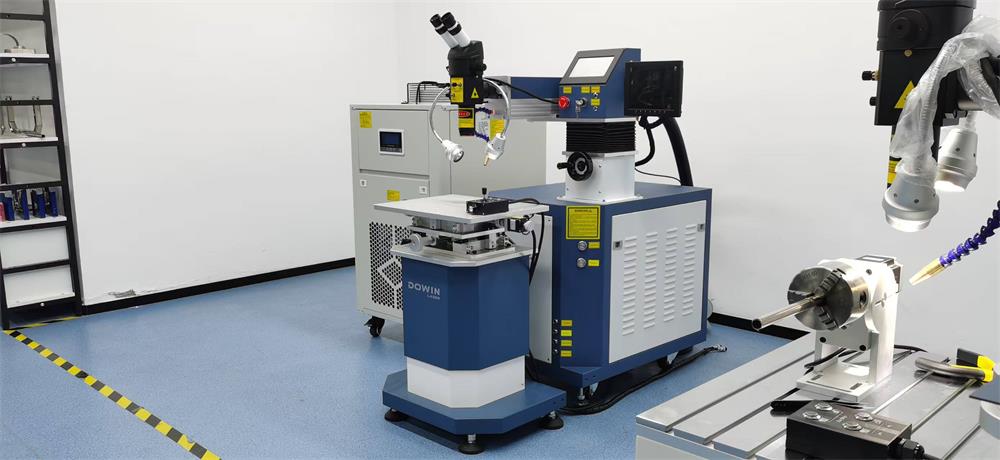
What Is a YAG Laser Welding Machine?
A YAG laser welding machine uses a Nd:YAG (Neodymium-doped Yttrium Aluminum Garnet) crystal to generate a 1064nm wavelength laser beam. The laser energy is focused onto microscopic welding areas, creating highly controlled melting without damaging surrounding PCB structures.
Unlike conventional soldering irons or wave soldering systems, YAG laser welding offers:
- Contactless processing
- Ultra-small heat affected zones
- High positioning accuracy
- Stable micro-welding capability
- Reduced oxidation
- Minimal PCB deformation
For PCB manufacturers dealing with miniaturized electronics, these advantages are becoming essential rather than optional.
Why YAG Laser Welding Is Ideal for PCB Boards
1. Extremely Precise Heat Control
One of the biggest problems in PCB assembly is thermal damage. Sensitive chips, capacitors, and ICs can fail when exposed to excessive heat.
YAG laser welding concentrates energy into a tiny focal spot, allowing manufacturers to weld specific points without affecting nearby components. This is especially important for:
- SMT assembly
- Fine-pitch IC packaging
- Flexible PCB welding
- HDI PCB production
- Sensor module assembly
Studies on laser soldering in electronics show that localized laser heating significantly reduces thermal stress on adjacent components.
2. Better Performance for Miniaturized Electronics
The electronics market is obsessed with miniaturization. Devices are becoming thinner, lighter, and more integrated every year.
Traditional soldering methods were designed for larger electronic structures. YAG laser systems were practically born for microelectronics.
Modern PCB production now involves:
- 0201 and 01005 components
- Flexible circuits
- Multilayer HDI boards
- Wearable electronics
- Medical PCB assemblies
Laser welding enables microscopic weld points with exceptional repeatability. In some advanced PCB laser processing applications, structure widths as small as 25 μm are achievable without damaging the substrate.
That level of precision fundamentally changes what manufacturers can build.
3. Non-Contact Welding Reduces Mechanical Stress
Traditional soldering tips physically touch PCB surfaces. Over time, this introduces:
- Mechanical wear
- Surface contamination
- Flux residue
- Pad lifting risks
YAG laser welding is completely non-contact. The laser beam transfers energy without physical pressure.
This matters enormously in fragile electronics manufacturing sectors such as:
- Aerospace electronics
- Medical equipment
- Automotive ECUs
- Optical communication modules
- MEMS sensors
The shift toward non-contact manufacturing is one of the hidden revolutions inside modern electronics production.
4. Cleaner and More Automated Production
Factories are under pressure to improve both production speed and environmental compliance.
Laser welding reduces:
- Consumable usage
- Flux dependency
- Post-cleaning operations
- Oxidation contamination
- Rework rates
At the same time, YAG laser systems integrate well with robotic automation and AI-driven inspection systems.
The future PCB factory will not look like the old soldering workshop. It will resemble a highly automated optical processing laboratory.
This transformation is already happening in advanced electronics manufacturing.
Main PCB Applications of YAG Laser Welding Machines
Surface Mount Device (SMD) Welding
Laser welding is extremely effective for small SMD components where solder bridges and overheating are common problems.
Flexible PCB Welding
Flexible PCBs are highly sensitive to thermal deformation. Laser welding minimizes substrate stress while improving joint consistency.
Sensor PCB Manufacturing
Modern automotive and industrial sensors require ultra-reliable micro-connections. YAG lasers offer stable, repeatable weld quality.
Battery Management Systems (BMS)
EV battery systems use highly complex PCB assemblies that demand strong conductivity and thermal reliability.
PCB Repair and Rework
Laser welding enables highly selective repair of damaged solder joints without affecting nearby circuitry.
This is one area where YAG technology still outperforms many traditional soldering systems.
YAG Laser vs Traditional Soldering
| Feature | YAG Laser Welding | Traditional Soldering |
|---|---|---|
| Heat Control | Extremely precise | Broad heat spread |
| Contact Method | Non-contact | Physical contact |
| PCB Damage Risk | Very low | Moderate to high |
| Suitable for Microelectronics | Excellent | Limited |
| Automation Compatibility | High | Medium |
| Oxidation Risk | Low | Higher |
| Flexible PCB Compatibility | Excellent | Difficult |
| Rework Precision | Very high | Moderate |
The industry trend is clear: as PCB density increases, laser-based joining technologies become increasingly valuable.
The Hidden Reason Electronics Factories Are Investing in Laser Welding
Most discussions about laser welding focus on precision. But the deeper reason factories are upgrading is economic survival.
Electronics manufacturers face four major pressures today:
- Rising labor costs
- Smaller component sizes
- Higher reliability standards
- Faster product cycles
Traditional soldering methods create bottlenecks in all four areas.
Laser welding reduces rework, improves consistency, enables automation, and supports next-generation PCB architectures simultaneously.
That combination is difficult to ignore.
Challenges of YAG Laser Welding in PCB Production
No technology is perfect.
YAG laser welding still has several limitations:
- Higher initial investment cost
- Requires trained operators
- Precision setup is critical
- Reflective materials can reduce efficiency
- Cooling systems are essential for stability
However, as electronics manufacturing becomes more advanced, these disadvantages are becoming easier to justify financially.
The cost of PCB failure is now far greater than the cost of precision welding equipment.
Future Trends of Laser Welding in PCB Manufacturing
The next five years will likely reshape PCB production completely.
Several trends are accelerating:
- AI-assisted laser welding inspection
- Fully automated microelectronics assembly
- Flexible and wearable PCB manufacturing
- Ultra-thin PCB processing
- Smart factory integration
- High-speed laser soldering systems
Researchers are already exploring laser-assisted rapid PCB prototyping and sustainable PCB reconfiguration technologies.
The old idea that PCB manufacturing belongs only to giant factories is disappearing. Laser systems are making high-precision production faster, cleaner, and more accessible.
Conclusion
YAG Laser Welding Machines are becoming one of the core technologies behind next-generation PCB manufacturing.
As electronic devices continue shrinking while performance expectations rise, traditional soldering methods increasingly struggle to meet modern production demands.
YAG laser welding delivers:
- Precision
- Low thermal impact
- High automation compatibility
- Better weld consistency
- Superior performance for microelectronics
For PCB manufacturers focused on future-proof production, laser welding is no longer just an upgrade. It is rapidly becoming a competitive necessity.
Post time: May-15-2026
